In Shanghai, Huawei made an announcement that caught the attention of the entire semiconductor industry.

For years, many experts believed Huawei's progress in advanced chip development would eventually slow down. Since 2019, the company has faced restrictions that prevented it from accessing the most advanced chipmaking equipment from ASML, the only company capable of producing the world's leading Extreme Ultraviolet (EUV) lithography machines.
The assumption seemed straightforward. Without access to the best manufacturing tools, Huawei would gradually fall further behind competitors such as TSMC, Intel, and Samsung.
Instead, Huawei arrived with a very different message.
The company claims it has developed a new chip design approach called Logic Folding, a method that could potentially extend computing performance without relying solely on ever-smaller transistors.
If these claims hold up under independent verification, this may be more than a workaround for sanctions. It could represent an important new chapter in how chips are designed.
The Problem With Traditional Scaling
To understand why Logic Folding matters, we first need to understand the challenge facing the semiconductor industry.
For more than sixty years, progress in computing has followed a pattern commonly known as Moore's Law. Gordon Moore observed that the number of transistors on a chip roughly doubled every two years. As transistors became smaller, chips became faster, cheaper, and more powerful.
This approach transformed computing.
Early computers filled entire rooms and performed only a few thousand operations per second. Today, a smartphone contains billions of transistors and performs trillions of operations every second.
For decades, the industry achieved these gains by repeatedly shrinking transistor size.
However, this strategy is approaching its limits.
A transistor is essentially an electrical switch. Making it smaller allows more transistors to fit onto a chip while also helping the transistor switch faster. But there is a hidden problem.
The wires connecting those transistors also become smaller.
As wires shrink, their electrical resistance increases. Signals take longer to travel through them, creating delays across the chip. At advanced manufacturing nodes, the delay caused by wiring can become much larger than the delay inside the transistor itself.
There is also a more fundamental challenge.
As transistors approach atomic dimensions, electrons can begin to tunnel through barriers that are supposed to block them. At that point, the transistor stops behaving like a reliable switch.
This is one reason why processor clock speeds have remained largely between 3 and 4 GHz for many years, even though transistor counts continue to increase.
The industry has become extremely good at making things smaller. The question now is whether making things smaller is still the best path forward.
From Moore's Law to the τ Scaling Law
Huawei's announcement is not only about a new chip architecture. It is also about a new way of measuring progress in semiconductors.
For decades, the industry focused on transistor density as the primary measure of advancement. Huawei argues that this approach is running into both economic and physical limits.
Instead of focusing only on how many transistors can fit onto a chip, Huawei proposes what it calls the τ (tau) Scaling Law.
In engineering, τ represents a time constant. Put simply, it measures how quickly signals move through a system. Huawei believes future computing performance will increasingly depend on reducing delays across the entire computing stack rather than only shrinking transistors.
This represents a shift in thinking.
Moore's Law focused on optimizing space. Huawei's τ Scaling Law focuses on optimizing time.
The company says it has already mass-produced hundreds of chip designs based on τ Scaling principles. However, the upcoming Kirin processors will be the first flagship smartphone chips to fully showcase Logic Folding as a practical implementation of this new approach.
The objective is straightforward. If data, instructions, and signals can move faster throughout the system, overall performance, energy efficiency, and transistor density can improve together.
A Different Way of Thinking
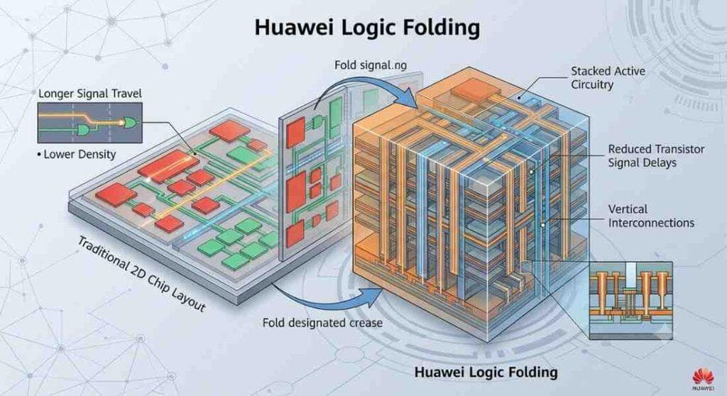
Huawei's Logic Folding starts with a different assumption.
Instead of focusing only on reducing transistor size, the company focuses on reducing the distance signals need to travel inside a chip.
Traditional chips are designed like a large single-story factory. Components are spread across a flat surface, and signals move horizontally between them.
Logic Folding turns that factory into a multi-story building.
Instead of placing everything side by side, layers of active circuitry are stacked vertically. Components that would normally be separated by long distances can now sit directly above or below each other.
The result is shorter communication paths and potentially faster operation.
Imagine two teams working on opposite sides of a football field. Communication naturally takes time. Now imagine placing those teams on different floors of the same building connected by an elevator. Communication becomes much quicker.
That is the basic idea behind Logic Folding.
Logic Folding Works Across Four Levels
One reason Huawei believes Logic Folding can deliver meaningful gains is that it does not focus on a single layer of chip design. Instead, it applies optimization across four different levels.
- Device Level: At the lowest level, Huawei optimizes transistor resistance and stray capacitance. The goal is to reduce the physical time constant τ and allow signals to move through the hardware more efficiently.
- Circuit Level: Traditional circuit layouts often require signals to travel long distances across a chip. Logic Folding redesigns these pathways by bringing critical components closer together and reducing resistive and capacitive loading. This helps improve circuit performance while increasing transistor density.
- Chip Level: Huawei combines software, architecture, and silicon design into a coordinated process. Rather than optimizing each layer independently, the company attempts to improve how instructions and data flow through the processor, reducing execution time and increasing efficiency.
- System Level: At the highest level, Huawei introduces a new interconnect approach called UnifiedBus. The goal is to create unified memory addressing and reduce communication delays between processors, memory, and computing clusters. This becomes increasingly important for AI workloads and large-scale computing systems.
Taken together, these four layers reflect Huawei's broader strategy. Instead of treating performance as a transistor problem, the company is trying to optimize the entire computing stack.
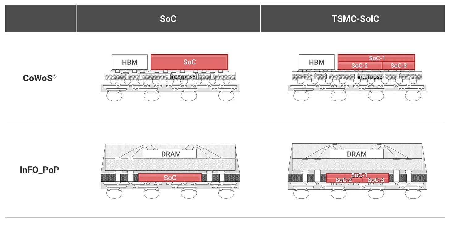
Why This Is Different From Existing 3D Chips
At first glance, Logic Folding sounds similar to existing 3D chip technologies.
Companies already stack memory chips on top of processors. Modern graphics cards use this approach to achieve extremely high memory bandwidth.
However, Huawei claims Logic Folding goes much further.
Traditional 3D stacking is largely a packaging technique. Engineers design chips as flat structures first and then stack them later.
Logic Folding introduces the vertical dimension much earlier in the design process.
The chip is designed from the beginning with vertical connections in mind. Critical signal paths are intentionally folded into three dimensions to reduce delays.
This makes Logic Folding more of an architectural shift than a packaging improvement.
The Numbers Huawei Presented
Huawei's claims are ambitious.
According to figures presented during private briefings, the company's previous generation chips achieved around 155 million transistors per square millimeter.
Its upcoming Kirin 2026 processor is expected to reach approximately 238 million transistors per square millimeter.
That represents a 53 percent increase in density within a single generation.
For comparison, TSMC's advanced N2 process is estimated to achieve around 292 million transistors per square millimeter.
Huawei remains behind the industry's leading edge, but the gap appears much smaller than many expected, especially considering the manufacturing restrictions the company faces.
The company also claims several additional benefits:
- 50 percent fewer clock buffers
- 25 percent lower clock skew
- Shorter data paths throughout the chip
- Improved power efficiency
- CPU frequencies reaching 3.1 GHz today
- A roadmap targeting 5 GHz mobile-class processors by 2031
These are significant claims. If validated, they suggest that architectural innovation can partially compensate for limitations in manufacturing technology.
The Challenges Are Still Huge
Despite the excitement, there are important reasons for caution.
The first challenge is software.
Modern chips are designed using Electronic Design Automation (EDA) tools. These tools were built around decades of two-dimensional design principles.
Logic Folding requires engineers to think in three dimensions, which means many existing design tools must evolve as well.
The second challenge is heat.
Heat management is already one of the biggest problems in semiconductor design. Stacking active circuitry on top of itself makes cooling significantly harder.
Removing heat from the center of a multi-layer chip is much more difficult than cooling a flat design.
Huawei itself has acknowledged that thermal management remains one of the largest challenges on its roadmap.
Ultimately, the success of Logic Folding may depend less on whether the concept works and more on whether heat can be managed effectively at scale.
The Bigger Story
Many people view this announcement primarily through a geopolitical lens.
The simple narrative is that Huawei found a way around export restrictions.
There is some truth to that view, but it may not be the most interesting part of the story.
The semiconductor industry already knew that traditional transistor scaling would eventually slow down. Even the world's most advanced lithography systems cannot shrink transistors forever.
At some point, physics becomes the limiting factor.
What makes Huawei's announcement noteworthy is that it points toward a different path forward.
Rather than asking how to make transistors smaller, Logic Folding asks how to make chips smarter in the way they are organized.
More importantly, Huawei is arguing that the future of semiconductor progress may come from reducing system-wide latency, represented by τ, rather than relying solely on transistor shrinkage.
Whether Huawei's implementation ultimately succeeds remains to be seen. Independent testing of future products will provide the real answer.
However, the underlying idea is based on sound engineering principles.
Interestingly, TSMC, Intel, and Samsung are also investing heavily in advanced 3D technologies. The difference is that they are pursuing these technologies from a position of abundance, with access to the world's best manufacturing tools.
Huawei is pursuing them from a position of constraint.
History has often shown that scarcity can drive innovation in unexpected directions.
If Logic Folding performs as advertised, it may be remembered not simply as Huawei's response to sanctions, but as an early glimpse into how the semiconductor industry evolves after Moore's Law reaches its limits.
That possibility alone makes this development worth paying attention to.